Sunday, August 22, 2010

experiment 8

Vary base resistor and measure the changes in voltage and current for vce,vbe, ic & ib.


I chose 5 different value resistors as shown in diagram on the left.                                                 What happened to the vce during this experiment was there is more current flow through due to bigger resistors.                                                   What happened to vbe during same experiment was only a small vd due to different size resistors.        What happened to Ib was that the current flow changed due to the different size resistors being used in the circuit.                                                       What happened to Ic the voltage rose as the gate was opened up because the flow through Ib was greater.     
Calculating the BETA (Hfe) of this transistor using the above graph.the Ratio between Collector over Base.......   
(1) 3.1 / 5 mA
(2) 5 / 4.37 mA
(3) 5 / 1 mA
(4) 104 / 21.7 mA
(5) 5.1 / 4.5 mA
Explaination of the line graph and what it is telling me.
The saturated region on the graph is the ideal place to be showing that the transistor is using minimal voltage but is creating high amps.
The active region is where you would expect a good working transistor to be, it functions using high voltage and still has the good amperage flow.
The cut off region is where the transistor isn't working well, its using using high voltage and is preventing amps from flowing through.
                

Experiment 7

Components used... 1 small NPN transistor and 2 resistors

Connected the multi meter between base and emitter got a voltage reading of 0.7 v   and also recorded a high amp flow.
              Connected multi meter between collector and emitter got a reading of 0.6v indicating that the transistor is ewell saturated and is working well as a switch.
Demostrating how the transistor works...  A on the diagram to the left would indicate high current flow using low voltage shows that this is a good working switch.                                     B on the diagram is located on the bottom yu can just see it..shows low current flow using high voltage indicating a bad switch.
The power dissapated by the transistor at vce of 3v is 15 ic (ma) this is known as the active zone.

What is the Beta of this transitor at 2,3 & 4 v?

2 v = 20/.8 mA
3 v = 14/.5 mA
4 v = 5/.2 mA

Experiment 6 meter checking of transistor.

When testing B.J.T (bipolar junction transistor) you switch the multi meter to diode test mode, you would perform this test to find out which is the BASE COLLECTOR and EMITTER.

There are 2 types... the PNP and the NPN type

To check BJT you would first measure using multi meter on the diode setting to find out which is PNP and NPN once you distinguish which is which you would then easily find the base...collector and emitter...the emitter base juntion usually has a higher forward VD. This is due to the difference in the doping concentration between the emitter and collector of the BJT.

experiment 5 Capacitors

Capacitors consist of 2 metal plates that are positioned close to each other but are seperated by insulator and when connected to an external power source electrons flow into the negative plates and thus charges up the capacitor, this charge remains in capacitor even once the power source has been removed, depending on the size of capacitance of the capacitor.... larger capacitors obviously hold and store more charge than a smaller 1.
Here are a couple of the smaller type capacitors commonly used. When using capacitors you must make sure to check whether or not it has a negative side to it. This can be identified by a - symbol.
Here are a couple more different type capacitors the - side of these particular capacitors is easily identified by the shorter leg of the 2.
The size of a capacitor is identified by the "farad" that is commonly printed on the capacitor itself. If "Farad" cant be found  you can also check to see if EIA code is listed.
below are some examples of different capacitors and there charging times with added resistance. This charging time is shown by the amount of V used to charge and the MS it takes to become fully charged along with the resistance being used.

Thursday, August 5, 2010

circuit board 1...


..COMPONENTS USED..
1x circuit board
2x 1k ohms resistors
2x 560 ohms resistors
1x 5v  (LED) yellow
1x 5v (LED) green
2x c547 B.J.T
plus jumper and power + earth wires


This circuit board i made is based on an injector circuit, using bi polar juntion transistors to amplify signal from ECU.
This particular circuit uses both a 5v and 12v input,.The resistors i used are a simple current flow control device.
A 12v current supply is sent to the collector of (bjt) and 5v to the base which in return lets current flow from the collector to emitter then to ground.
VD (voltage drop) was measured across all components with the following results..

R13 = 6.60v
R14 = 10.4v
R15 = 10.1v
R16 = 6.72v
LED (green) = 2.50v
LED (yellow) = 2.55v
V-CE = 0.05v
V-CE = 0.05v
V-BE = 0.88v
V-BE = 0.88v

These results were what was expected and this circuit board worked exactly how it was intended to.

Monday, August 2, 2010

Experment 4

This experiment was done using a breadboard, muliti meter, a 12v adjustable power supply 1x resistor 1k.ohm, 1x 5v1 zener diode, and 1x diode 1N4007.


Once I had completed building my circuit i did a range of tests at 10v and 15v 

At 10v the voltage drops are as recorded ..
Vd across zener diode 4.68v
Vd across diode .65v
Vd across both zener diode and diode 5.34v
Vd across resistor 4.87v

10v 4.87 / 1000
=0.00487a

the calculated current for this circuit at this voltage is 0.00487a using ohms law.

At 15v the voltage drops are as recorded..
Vd across zener diode 4.83v
Vd across diode .68v
Vd across both zener diode and diode 5.52v
Vd across resistor 9.11v
15v  9.11 / 1000
=0.00911a

          the calculated current for this circuit at this voltage is 0.00911a using ohms law.                
  
What is happening here is that because the value of both the zener diode and diode is 5v the calculated Vd is similar at both voltage settings.


Experiment 3

This experement was done using a multi meterbread board ,2x resistors a 5v1 zener diode and a 12v power supply.

The resistors both have a value of 100 ohms
and Vs is 12v given the Vz over the zener diode to be 4.96v.
We then had to vary the power supply form 10v - 15v monitoring the value of Vz this was recorded at 4.84v at 10v Vs and climbed to 5.02v at 15v Vs..this would be expected as the zener diodes value is 5v if the reading was for example 7v over the zener this would indicate a short or open circut.
This cicuit could be used to regulate voltage.

If i was to reverse the polarity of the zener diode the value of Vz would be around .6 to .7 as this is the voltage required for the zener to start operating.

Sunday, July 25, 2010

experiment 2 "Diodes"

THIS DIAGRAM SHOWS THE OPERATION OF A BRIDGE RECTIFIER AS IT CONVERTS AC TO DC

DIODES TAKE 0.7V TO BECOME ACTIVE IF YOU PERFORM A V/D ACROSS DIODE AND FOR EXAMPLE IT READS
O.V THIS WOULD INDICATE A SHORT


In order to identify the ANODE and CATHODE this would normally be identafiable by a bar going around the diode.

A diode has the characteristics of a INSULATOR when current tries to flow in the 1 direction or a CONDUCTOR when the current flows in the other. 

The Anode end is represented by the + sign and the Cathode by the - sign in the diagrams provided above 


Below is the LIGHT EMMITING DIODE more commonly known as the L.E.D
                                                                            
L.E.Dz are reasonabally easy to distinguish the difference between the Anode Cathode sides..the Cathode side generally has a shorter leg to the Anode,.

experiment 1 "RESISTORS"

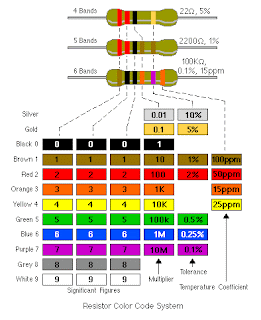
                                                   RESISTOR COLOUR CODE CHART

Demonstrating an understanding of resistors and there values...this is made easy by the use of the colour chart and a multi meter....

 A commonly asked ? is which end you start to read the band from this is easy if there is a gold or silver band at either end if there isn't one you would start at the side that is grouped up closely together if there is this means you keep that colour to the right and start reading  from the left..The gold and silver bands represent ..tolerance and co-efficiency.

When the resistors are put into a series there values can be added together to create a greater resistance level basically you just add the resistances together to get total resistance level.

But when put into a parralel connection for example if i had 3 resistors
A 100 ohms
B 235 ohms
C 220 ohms
this would be calculated as below

1/rt = 1/100 + 1/235 + 1/220 = 0.018

1/rt = 1/0.018

RT = 53.1 ohms

This has given you a total resistance level of 53 ohms which is correct as it should be lower than the lowest resistor used.

I tested  6 different resistors and applied this formula above to determine there values in parallel and series connections.


For example a resistor with

3 BANDS

ORANGE-ORANGE-BROWN has a value of   (330 ohms)

4 BANDS

RED-YELLOW-ORANGE-GOLD has a value of (24k-ohms 5%)

5 BANDS

RED-YELLOW-ORANGE-BLACK-BROWN

But if you come across a resistor with 5 bands for example

BROWN-YELLOW-BLACK-GOLD-RED

This resistor is calculated with the 4band rule ignoring the red.